
Published 2023. 1. 13. 16:51
1. 2023.01.16 ( 월 )
PCH,clk 수정
1.1. PCH신호 수정
PCH신호 생성을 위한 module을 삭제하고 일반 D F/F를 사용하여 ME신호 5ns후에 반응하도록 한다.

1.2. Final module CODE
//----------negedge clk D ff ---------
module negedge_Dff(q,din,clk,rst);
input din,clk,rst;
output reg q;
always @(negedge rst or negedge clk) begin
if(rst==0 )
q<=0;
else
q<=din; end
endmodule
//----------posedge clk D ff---------
module posedge_Dff(q,din,clk,rst);
input din,clk,rst;
output reg q;
always @(negedge rst or posedge clk) begin
if(rst==0 )
q<=0;
else
q<=din;
end
endmodule
//------------------SL 신호-----------------
module SL_signal(SL_in,S0,S1,S2,S3,S_B0,S_B1,S_B2,S_B3);
input [0:3] SL_in;
output reg S0,S1,S2,S3,S_B0,S_B1,S_B2,S_B3;
always @(SL_in) begin
if (SL_in[0]==1) S0=0;
else if(SL_in[0]==0) S0=1;
if (SL_in[1]==1) S1=0;
else if(SL_in[1]==0) S1=1;
if (SL_in[2]==1) S2=0;
else if(SL_in[2]==0) S2=1;
if (SL_in[3]==1) S3=0;
else if(SL_in[3]==0) S3=1;
S_B0= ~S0; S_B1= ~S1; S_B2= ~S2; S_B3= ~S3; end
endmodule
module SL_output(timing,SL_temp,SL_B_temp, SL,SL_B);
input timing,SL_temp,SL_B_temp;
output reg SL,SL_B;
always@(timing) begin
if(timing==1) begin
SL=SL_temp;
SL_B=SL_B_temp; end
else begin
SL=0;
SL_B=0; end
end
endmodule1.3. TESTBENCH CODE
module testbench();
reg clk,rst,ME;
always begin
clk=~clk;
#5;
end
wire PCH,PCH_b;
negedge_Dff dff1(PCH,ME,clk,rst);
not(PCH_b,PCH);
wire sl_timing,se;
reg [0:3] SL_in;
posedge_Dff dff4(sl_timing,PCH,clk,rst);
negedge_Dff dff5(se,sl_timing,clk,rst);
wire SL0_temp,SL1_temp,SL2_temp,SL3_temp,SL_B0_temp,SL_B1_temp,SL_B2_temp,SL_B3_temp;
wire SL0,SL1,SL2,SL3,SL_B0,SL_B1,SL_B2,SL_B3;
SL_signal SL_siganl1(SL_in,SL0_temp,SL1_temp,SL2_temp,SL3_temp,SL_B0_temp,SL_B1_temp,SL_B2_temp,SL_B3_temp);
SL_output SL_output0(sl_timing,SL0_temp,SL_B0_temp,SL0,SL_B0);
SL_output SL_output1(sl_timing,SL1_temp,SL_B1_temp,SL1,SL_B1);
SL_output SL_output2(sl_timing,SL2_temp,SL_B2_temp,SL2,SL_B2);
SL_output SL_output3(sl_timing,SL3_temp,SL_B3_temp,SL3,SL_B3);
initial begin ME=0; rst=0; SL_in=4'b0011; clk=0;
// i1=4'b0001; i2=4'b0010; i3=4'b0100; i4=4'b1000;
#5 ME=1; rst=1;
#35
$finish;
end
endmodule1.4. Simulation
1.5. PCH신호 재설계
내가 너무 코딩을 기준으로 신호를 설계한 것 같다. 따라서 순차회로 설계방식으로 다시 설계하였다
위와 같은 과정으로 신호를 만들었고 식을 만들어 회로를 설계하였다.
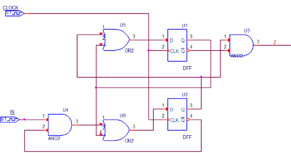
1.5.1. PCH 신호 모듈
module PCH(x,z,clk,rst);
input x,clk,rst;
output z;
wire d1,d2,d22,q2_not,q1,q2,q1_not;
//q1,q2 q1'q2'
not(q2_not,q2);
not(q1_not,q1);
//d1 gate 연결
or(d1,q1,q2);
//d2 gate 연결
and(d2,x,q2_not);
or(d22,d2,q1);
//z gate연결
and(z,q1_not,q2);
negedge_Dff dff1(q1,d1,clk,rst);
negedge_Dff dff2(.q(q2),.din(d22),.clk(clk),.rst(rst));
endmodule1.6. Simulation
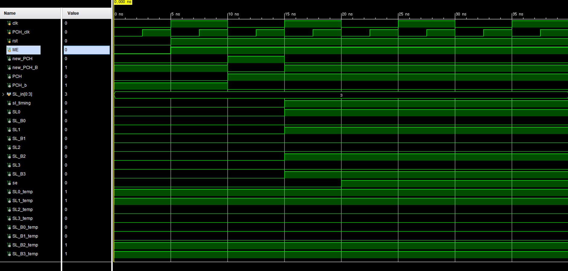
edge기준으로 설계한 베릴로그는 FPGA연결시 위험할 수 있다. 따라서 회로 기준으로 설계를 하였고 그 결과 위와 같이 성공적으로 결과가 나왔다. 야호
2. 2023.01.18 ( 수 )
-연구실에 왁스칠하는 날. 연구실 휴무!
3. 2023.01.20 ( 금 )
선배가 시간표 봐주심..
시간표랑 졸업조건,설계과목 등 계획함.
'feram control signal 연구일지' 카테고리의 다른 글
| 5주차 ( 2023.01.23~2023.01.27 ) FPGA 연결 (0) | 2023.01.27 |
|---|---|
| 3주차 ( 2023.01.09~2023.01.13 ) (0) | 2023.01.11 |
| 2주차 (2023.01.02~01.6) (0) | 2023.01.04 |
| 1주차 (2022.12.26~ 12.30) (0) | 2022.12.28 |